

1 / 5
PET Bottle Making Machine is suitable for producing PET plastic containers and bottles in all shapes.
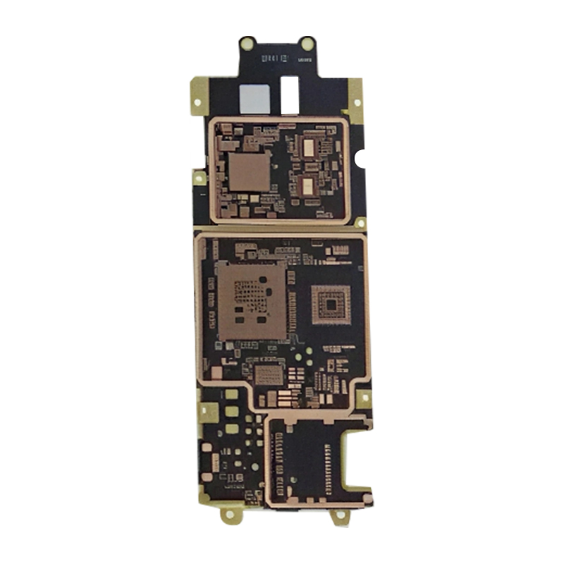
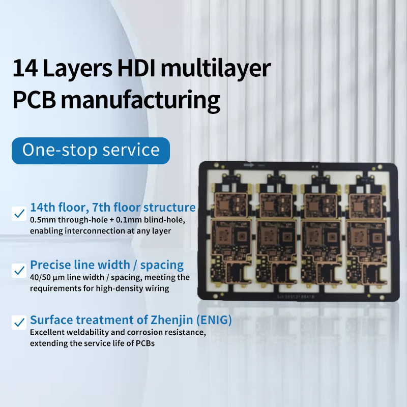
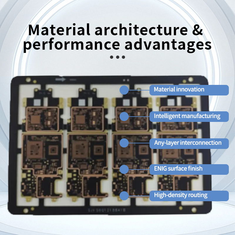
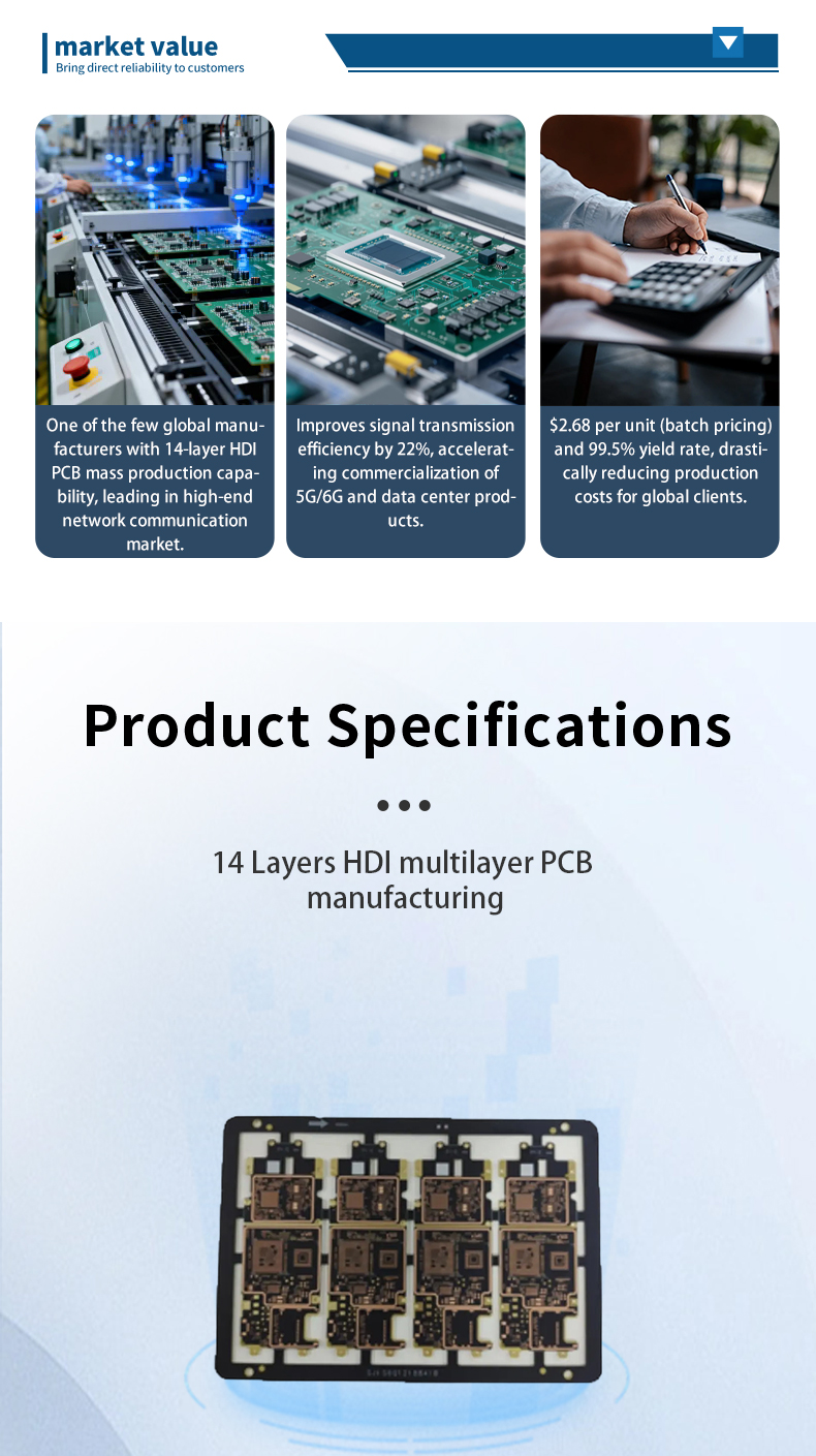
| Product Name | Network Communication PCB |
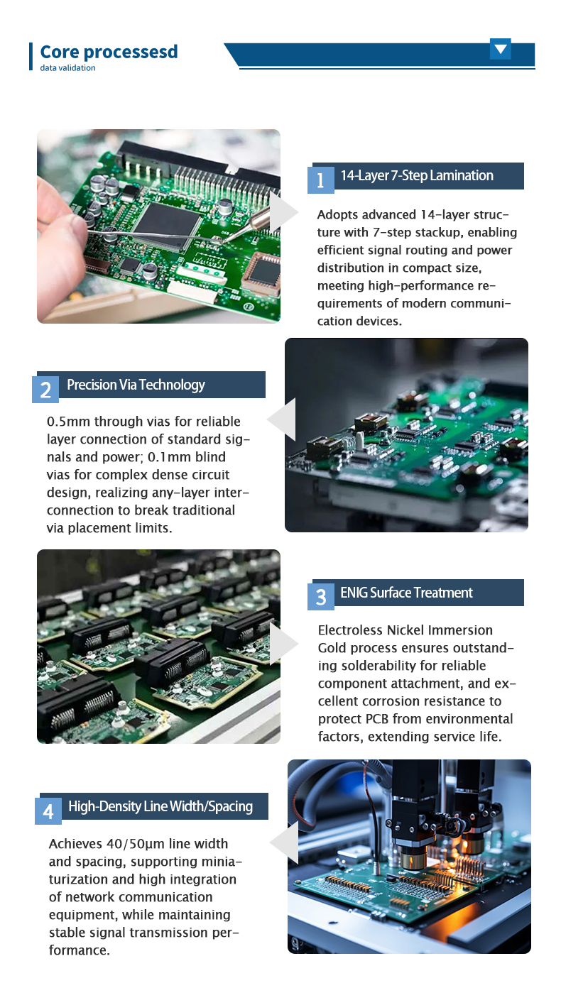
| Number of Layers | 14 layers, 7 steps (referring to the layer stack-up configuration) |
| Board Thickness | 0.85mm |
| Dimensions | 130.5*111.6mm |
| Material | Taiyo EM390, 0.05mm (likely referring to the copper clad laminate material with a specific thickness or model number) |
| Thickness Ratio | 1.56:1 |
| Minimum Aperture | Through-hole: 0.5mm; Blind via: 0.1mm |
| Minimum Trace Width/Spacing | 40/50μm |
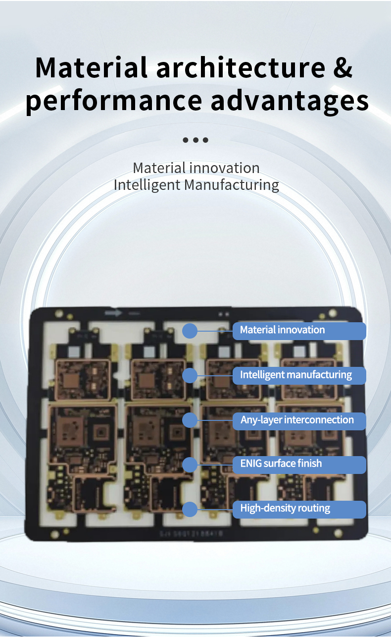
| Product Features | Any-layer interconnection |
| Surface Treatment Type | Immersion Gold (ENIG) |
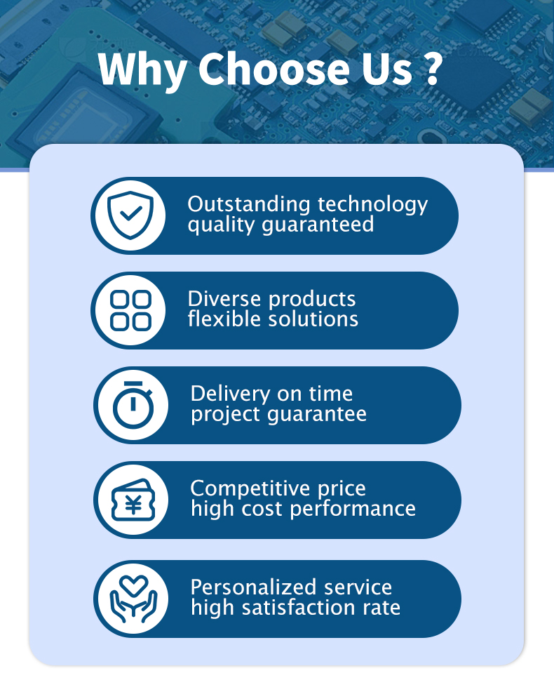

We lead in PCB manufacturing with advanced processes like high-precision drilling, fine-line fabrication (min. 50μm line width/spacing), and multi-layer lamination, meeting high-end routing density needs for stable signal transmission. A strict quality system ensures over 99.5% yield via flying probe and AOI tests. Our expert R&D team offers tailored solutions, from material selection to complex circuit design.
We provide FR-4, high-frequency, metal-core, and flexible boards, each with unique properties for various applications. Mass-produce 2 - 30 layer PCBs for efficient signal and power management. Customize board size, hole diameter, surface finish, and functions to fit specific scenarios.
Optimized production and advanced management shorten cycles. We control delivery for double-sided PCBs within [X] days and arrange multi-layer PCBs flexibly. With large capacity and emergency response, we avoid delays. Real-time tracking keeps clients informed.
Cost-saving measures enable competitive pricing without compromising quality. Transparent quotes detail all costs. Our PCBs excel in price, quality, and delivery, enhancing clients' product competitiveness.
Our sales team offers pre-sales expertise. Technical support spans design to production. We handle after-sales issues promptly and conduct follow-ups for continuous improvement.
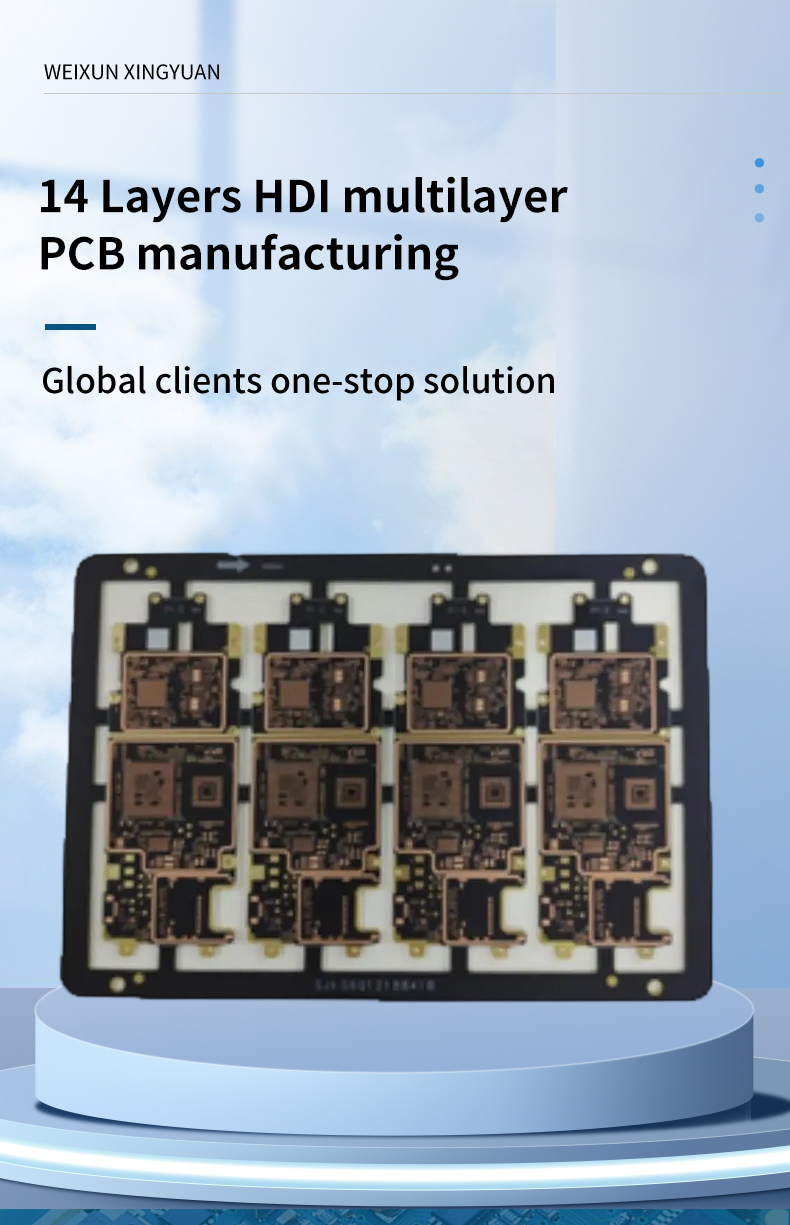
The Network Communication PCB is a 14-layer board with a thickness of 0.85mm and dimensions of 130.5*111.6mm. It is built using Taiyo EM390 material (0.05mm), featuring a 1.56:1 thickness ratio, a minimum through-hole aperture of 0.5mm, and a minimum trace width/spacing of 40/50μm.
By utilizing 0.1mm blind vias, signals can be routed directly between any two layers without being restricted by traditional via placement rules. This greatly increases design flexibility and improves the electrical performance of the PCB within a compact space.
Immersion Gold (ENIG) offers excellent solderability, ensuring reliable component attachment during assembly. It also provides robust corrosion resistance, protecting copper traces from environmental factors and extending the board's operational life.
We supply 2 to 30 layer PCBs using versatile materials, including standard FR-4, high-frequency, metal-core, and flexible boards, to support different power and signal management requirements.
We implement a strict quality control system with advanced testing techniques, including flying probe and Automated Optical Inspection (AOI) tests, maintaining a yield rate of over 99.5%.
Our optimized production cycles control double-sided PCB deliveries within a standard [X]-day timeframe, while multi-layer PCB production schedules are arranged flexibly based on project requirements to ensure timely delivery.